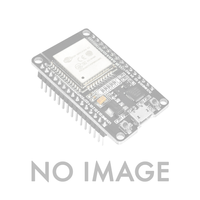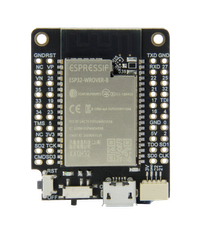
ESP32-WROOM Development Board Pinout and Technical Specifications
Code name: ESP32_WROOM_DA
ESP32-WROOM development board is based on esp32 microcontroller and uses xtensa architecture. This development board has a maximum CPU frequency of 240 MHz and a flash size of 4MB.
🔗 Quick Links

📝 ESP32-WROOM Description
The ESP32-WROOM-32 is a versatile and powerful Wi-Fi + Bluetooth® + Bluetooth LE module, designed to support a wide range of applications. It is equally suitable for low-power sensor networks as well as high-demand tasks like voice encoding, music streaming, and MP3 decoding.
At the heart of the module is the ESP32-D0WDQ6 chip, engineered for scalability and adaptability. This chip features two CPU cores that can be independently controlled, with an adjustable clock frequency ranging from 80 MHz to 240 MHz. Additionally, it includes a low-power coprocessor, which is ideal for handling tasks that require minimal computing power—such as peripheral monitoring—while conserving energy.
The ESP32 integrates a rich set of peripherals, including capacitive touch sensors, an SD card interface, Ethernet, high-speed SPI, UART, I2S, and I2C. Its combination of power, flexibility, and connectivity makes the ESP32-WROOM-32 a perfect choice for a broad spectrum of IoT and embedded applications.
📊 ESP32-WROOM Specs
Below you can find the specifications of ESP32-WROOM, such as features, connectivity options, and ESP32-WROOM technical specs.
✨ Features
- 40 digital IO pins
- 16 external interrupt pins
- 16 analog input pins
- 19 PWM pins
🛰️ Connectivity
- WiFi: 802.11 b/g/n (2.4 GHz)
- Bluetooth: 4.2
- BLE: 4.2
📐 Technical specs
| Microcontroller | esp32 |
| Clock Speed | 240 MHz |
| Flash size | 4MB |
| Architecture | xtensa |
🔌 ESP32-WROOM Pinout
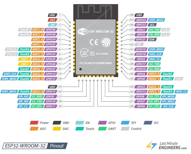
The ESP32-WROOM pinout is designed to offer developers a highly versatile and feature-packed layout for a variety of IoT and embedded applications. The ESP32 WROOM includes essential power pins such as 5V, 3.3V, and GND, ensuring stable power delivery for external components. Key communication protocols are well-supported, with pins for UART (RXD0, TXD0), SPI (MISO, MOSI, SCK, and SS), and I2C (SDA and SCL) to interface with a wide range of peripherals.
The ESP32 WROOM Devkit also supports multiple ADC pins (IO34, IO35, IO36, etc.), making it ideal for projects that require analog input, such as reading sensor data. Additionally, specialized pins such as DAC (IO25, IO26) and Touch Pins enhance its usability in advanced applications. The inclusion of RTC GPIOs further adds low-power features, allowing developers to take full advantage of the ESP32-WROOM pinout for efficient power management.
⚠️ Pins to Avoid or Use with Caution
Some pins are reserved for critical functions like bootstrapping, JTAG debugging, USB communication, and flash memory operations. Misusing these pins may lead to boot failures, programming issues, USB conflicts, or disruptions in flash storage. Below is a list of pins to avoid or use with caution, categorized for clarity:
- 🛠️ Strapping Pins (Boot Mode & System Behavior) - These pins control boot behavior and flash voltage selection. Pulling them high or low at reset can impact boot mode selection, voltage settings, or debugging access. Avoid altering their state unless necessary.
- 🔗 JTAG Debugging Pins - JTAG is used for low-level debugging and programming. If JTAG is enabled, these pins must remain dedicated to it. Repurposing them as GPIO can disable JTAG debugging features.
- 🔌 USB Communication Pins - These pins are used for USB Serial/JTAG communication. If USB debugging or communication is required, they should not be reassigned as GPIO.
- ⚡ Flash Memory & SPI Pins - Certain GPIOs are hardwired to SPI flash memory and PSRAM. Using them as standard GPIOs may result in system instability, corrupted storage, or boot failure.
- 📡 UART Serial Communication Pins - By default, these pins are used for serial debugging, console output, and firmware uploads. Repurposing them for general I/O may break UART programming or debugging capabilities.
| PIN | Label | Reason | Function |
|---|---|---|---|
| IO34 | GPIO34 | Cannot be used as output (no drive capability); only suitable for analog/digital input. | 🪛 Other |
| IO35 | GPIO35 | Cannot be used as output; only suitable for input. | 🪛 Other |
| IO14 | MTMS (GPIO14) | Used for JTAG debugging (TMS); driving it as GPIO may interfere with JTAG or produce spurious signals at boot. | 🪛 Other |
| IO12 | MTDI (GPIO12) | Keep LOW during boot (internal PD); pulling HIGH at reset selects 1.8V flash mode, causing flash brownout if 3.3V flash is used. | 🛠️ Strapping |
| IO13 | MTCK (GPIO13) | Used for JTAG debugging (TCK); avoid using as GPIO if JTAG is needed. | 🪛 Other |
| IO15 | MTDO (GPIO15) | Keep HIGH during boot (internal PU); if LOW on reset, bootloader log is silenced and boot mode may change. | 🛠️ Strapping |
| IO2 | GPIO2 | If driven HIGH on reset (while IO0 is LOW), selects an unsupported SDIO boot mode, causing boot failure. | 🛠️ Strapping |
| IO0 | GPIO0 | Must be HIGH during boot for normal startup; if held LOW on reset, forces flash programming mode. | 🛠️ Strapping |
| IO4 | GPIO4 | Sampled at reset for boot config; should not be driven at boot (affects boot mode timing). | 🛠️ Strapping |
| IO16 | GPIO16 | Connected to internal PSRAM on PSRAM-enabled modules; not usable as GPIO on those modules. | ⚡ Flash |
| IO17 | GPIO17 | Connected to internal PSRAM on PSRAM-enabled modules; not usable as GPIO on those modules. | ⚡ Flash |
| IO5 | GPIO5 | Must be HIGH during boot; if pulled LOW at reset, alters SDIO slave timing and may prevent normal boot. | 🛠️ Strapping |
📌 Key Takeaway:
- Before using any GPIO, check if it is assigned a critical function.
- Avoid using bootstrapping pins unless you're modifying boot behavior intentionally.
- If JTAG debugging is needed, ensure its pins remain free.
- USB and Flash-related GPIOs should remain dedicated unless you disable their default functions.
✅ Pins Safe to use
- 🔹 SENSOR_VP
- 🔹 SENSOR_VN
- 🔹 IO32
- 🔹 IO33
- 🔹 IO25
- 🔹 IO26
- 🔹 IO27
- 🔹 SHD/SD2
- 🔹 SWP/SD3
- 🔹 SCS/CMD
- 🔹 SCK/CLK
- 🔹 SDO/SD0
- 🔹 SDI/SD1
- 🔹 IO18
- 🔹 IO19
- 🔹 NC
- 🔹 IO21
- 🔹 RXD0
- 🔹 TXD0
- 🔹 IO22
- 🔹 IO23
Unlike restricted pins, these GPIOs are not tied to essential system functions like 🛠️ bootstrapping, 🔌 USB communication, 🔗 JTAG debugging, or ⚡ SPI flash memory, making them the best choices for custom applications and general use.
Why Are These Pins Safe?- Not involved in bootstrapping → These GPIOs do not affect the device’s boot mode or system startup.
- Not linked to flash memory or PSRAM → They won’t interfere with storage or memory access.
- Not dedicated to USB or JTAG → They remain free for general use without affecting debugging or programming.
- No special hardware connections → Unlike some pins that are internally wired to system functions, these remain freely assignable.
🗺️ ESP32-WROOM External Pins Mapping Functions
Below you can find the ESP32-WROOM pinout. This development board provides 40 digital IO pins, out of which 16 can be used as an external interrupt pins , 16 as analog input pins and 19 pins have Pulse-Width Modulation (PWM) .
| Pin | Function | ESP Pin | Input/Output | Description |
|---|---|---|---|---|
| 1 | SENSOR_VP | GPIO36 | input | ADC1_CH0, RTC_GPIO0 |
| 2 | SENSOR_VN | GPIO39 | input | ADC1_CH3, RTC_GPIO3 |
| 3 | IO34 | GPIO34 | input | ADC1_CH6, RTC_GPIO4 |
| 4 | IO35 | GPIO35 | input | ADC1_CH7, RTC_GPIO5 |
| 5 | IO32 | GPIO32 | bidirectional | XTAL_32K_P (32.768 kHz crystal oscillator input), ADC1_CH4, TOUCH9, RTC_GPIO9 |
| 6 | IO33 | GPIO33 | bidirectional | XTAL_32K_N (32.768 kHz crystal oscillator output), ADC1_CH5, TOUCH8, RTC_GPIO8 |
| 7 | IO25 | GPIO25 | bidirectional | DAC_1, ADC2_CH8, RTC_GPIO6, EMAC_RXD0 |
| 8 | IO26 | GPIO26 | bidirectional | DAC_2, ADC2_CH9, RTC_GPIO7, EMAC_RXD1 |
| 9 | IO27 | GPIO27 | bidirectional | ADC2_CH7, TOUCH7, RTC_GPIO17, EMAC_RX_DV |
| 10 | IO14 | GPIO14 | bidirectional | ADC2_CH6, TOUCH6, RTC_GPIO16, MTMS, HSPICLK, HS2_CLK, SD_CLK, EMAC_TXD2 |
| 11 | IO12 | GPIO12 | bidirectional | ADC2_CH5, TOUCH5, RTC_GPIO15, MTDI, HSPIQ, HS2_DATA2, SD_DATA2, EMAC_TXD3 |
| 12 | GND | N/A | power ground | Ground connection |
| 13 | IO13 | GPIO13 | bidirectional | ADC2_CH4, TOUCH4, RTC_GPIO14, MTCK, HSPID, HS2_DATA3, SD_DATA3, EMAC_RX_ER |
| 14 | SHD/SD2 | GPIO9 | bidirectional | SD_DATA2, SPIHD, HS1_DATA2, U1RXD |
| 15 | SWP/SD3 | GPIO10 | bidirectional | SD_DATA3, SPIWP, HS1_DATA3, U1TXD |
| 16 | SCS/CMD | GPIO11 | bidirectional | SD_CMD, SPICS0, HS1_CMD, U1RTS |
| 17 | SCK/CLK | GPIO6 | bidirectional | SD_CLK, SPICLK, HS1_CLK, U1CTS |
| 18 | SDO/SD0 | GPIO7 | bidirectional | SD_DATA0, SPIQ, HS1_DATA0, U2RTS |
| 19 | SDI/SD1 | GPIO8 | bidirectional | SD_DATA1, SPID, HS1_DATA1, U2CTS |
| 20 | IO15 | GPIO15 | bidirectional | ADC2_CH3, TOUCH3, MTDO, HSPICS0, RTC_GPIO13, HS2_CMD, SD_CMD, EMAC_RXD3 |
| 21 | IO2 | GPIO2 | bidirectional | ADC2_CH2, TOUCH2, RTC_GPIO12, HSPIWP, HS2_DATA0, SD_DATA0 |
| 22 | IO0 | GPIO0 | bidirectional | ADC2_CH1, TOUCH1, RTC_GPIO11, CLK_OUT1, EMAC_TX_CLK |
| 23 | IO4 | GPIO4 | bidirectional | ADC2_CH0, TOUCH0, RTC_GPIO10, HSPIHD, HS2_DATA1, SD_DATA1, EMAC_TX_ER |
| 24 | IO16 | GPIO16 | bidirectional | HS1_DATA4, U2RXD, EMAC_CLK_OUT |
| 25 | IO17 | GPIO17 | bidirectional | HS1_DATA5, U2TXD, EMAC_CLK_OUT_180 |
| 26 | IO5 | GPIO5 | bidirectional | VSPICS0, HS1_DATA6, EMAC_RX_CLK |
| 27 | IO18 | GPIO18 | bidirectional | VSPICLK, HS1_DATA7 |
| 28 | IO19 | GPIO19 | bidirectional | VSPIQ, U0CTS, EMAC_TXD0 |
| 29 | NC | N/A | not connected | No connection |
| 30 | IO21 | GPIO21 | bidirectional | VSPIHD, EMAC_TX_EN |
| 31 | RXD0 | GPIO3 | bidirectional | U0RXD, CLK_OUT2 |
| 32 | TXD0 | GPIO1 | bidirectional | U0TXD, CLK_OUT3, EMAC_RXD2 |
| 33 | IO22 | GPIO22 | bidirectional | VSPIWP, U0RTS, EMAC_TXD1 |
| 34 | IO23 | GPIO23 | bidirectional | VSPID, HS1_STROBE |
| 35 | GND | N/A | power ground | Ground connection |
🗺️ ESP32-WROOM Pins Mapping Arduino IDE
Below you can find the ESP32-WROOM pinout. This development board provides 40 digital IO pins, out of which 16 can be used as an external interrupt pins , 16 as analog input pins and 19 pins have Pulse-Width Modulation (PWM) .
| Pin | Analog | Touch | PWM | Other |
|---|---|---|---|---|
| 0 | A11 | T1 | ||
| 1 | PWM | TX | ||
| 2 | A12 | T2 | PWM | ANT1 |
| 3 | PWM | RX | ||
| 4 | A10 | T0 | PWM | |
| 5 | PWM | SS | ||
| 12 | A15 | T5 | PWM | |
| 13 | A14 | T4 | PWM | |
| 14 | A16 | T6 | PWM | |
| 15 | A13 | T3 | PWM | |
| 18 | PWM | SCK | ||
| 19 | PWM | MISO | ||
| 21 | PWM | SDA | ||
| 22 | PWM | SCL | ||
| 23 | PWM | MOSI | ||
| 25 | A18 | PWM | DAC1 ANT2 | |
| 26 | A19 | PWM | DAC2 | |
| 27 | A17 | T7 | PWM | |
| 32 | A4 | T9 | PWM | |
| 33 | A5 | T8 | PWM | |
| 34 | A6 | |||
| 35 | A7 | |||
| 36 | A0 | |||
| 39 | A3 |
🛠️ Default Tools
| Bootloader tool | esptool_py |
| Uploader tool | esptool_py |
| Network uploader tool | esp_ota |
| Bootloader address | 0x1000 |
| Flash mode | dio |
| Boot mode | dio |
| PSRAM type | |
| Maximum upload size | 1280 Kb (1310720 B) |
| Maximum data size | 320 Kb (327680 B) |
The ESP32-WROOM development board by default uses esptool_py uploader tool, esp_ota network uploader tool for Over-the-air (OTA) uploads and esptool_py bootloader tool. The bootloader starts at address "0x1000". Flash mode and boot mode for ESP32-WROOM development board by default is dio and dio respectively.