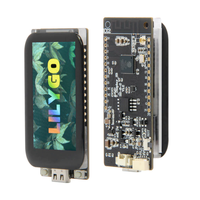
LilyGo T-Display-S3 Touch Development Board Pinout and Technical Specifications
Code name: LILYGO_T_DISPLAY_S3
Manufacturer: LilyGo
LilyGo T-Display-S3 Touch development board is based on esp32s3 microcontroller and uses xtensa architecture. This development board has a maximum CPU frequency of 240 MHz and a flash size of 16MB.
🔗 Quick Links
🛒 Price


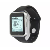
📝 LilyGo T-Display-S3 Touch Description
🚀 The LilyGo T-Display-S3 is a powerful development board featuring an ESP32-S3 chip with integrated WiFi and Bluetooth 5 capabilities. Equipped with a 1.9-inch LCD (270x320) driven by an ST7789V controller, it provides a vibrant display for embedded applications. ⚡
📡 With WiFi 802.11 b/g/n and Bluetooth 5 (LE), it offers seamless wireless connectivity for IoT projects. Its 8MB PSRAM and 16MB Flash memory ensure ample storage and performance.
💾 Designed with multiple GPIOs, PWM, ADC, I2C, and SPI support, it is suitable for various applications, including sensor interfacing, graphical user interfaces, and wireless communication.
📊 LilyGo T-Display-S3 Touch Specs
Below you can find the specifications of LilyGo T-Display-S3 Touch, such as features, connectivity options, and LilyGo T-Display-S3 Touch technical specs.
✨ Features
- 13 digital IO pins
- 13 external interrupt pins
- 10 analog input pins
- 13 PWM pins
🖥 Display
- Type: LCD
- Size: 1.9"
- Resolution: 170x320
🖥️ Display
- Type: LCD
- Size: 1.9"
- Resolution: 170x320
🛰️ Connectivity
- WiFi: 802.11 b/g/n (2.4 GHz)
- Bluetooth: 5.0
- BLE: 5.0
📐 Technical specs
| Microcontroller | esp32s3 |
| Clock Speed | 240 MHz |
| Flash size | 16MB |
| PSRAM Size | 8MB |
| Architecture | xtensa |
🔌 LilyGo T-Display-S3 Touch Pinout
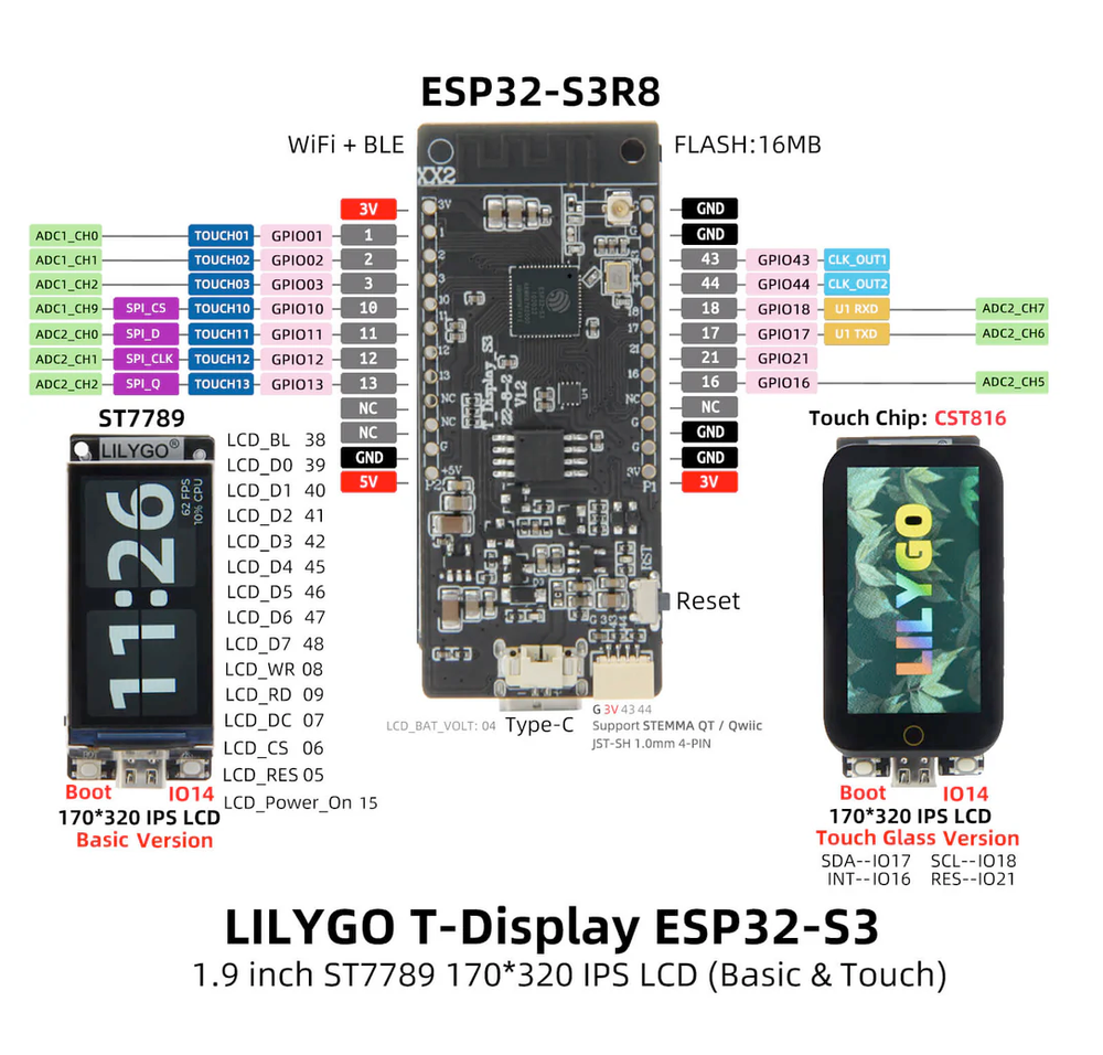
The LilyGo T-Display-S3 pinout provides various digital and analog pins, along with a dedicated display interface. Key pins include:
5V and 3.3V power rails for stable operation.
SDA and SCL for I2C, MISO, MOSI, SCK, and SS for SPI communication.
Additionally, dedicated LCD pins ensure efficient display control.
⚠️ Pins to Avoid or Use with Caution
Some pins are reserved for critical functions like bootstrapping, JTAG debugging, USB communication, and flash memory operations. Misusing these pins may lead to boot failures, programming issues, USB conflicts, or disruptions in flash storage. Below is a list of pins to avoid or use with caution, categorized for clarity:
- 🛠️ Strapping Pins (Boot Mode & System Behavior) - These pins control boot behavior and flash voltage selection. Pulling them high or low at reset can impact boot mode selection, voltage settings, or debugging access. Avoid altering their state unless necessary.
- 🔗 JTAG Debugging Pins - JTAG is used for low-level debugging and programming. If JTAG is enabled, these pins must remain dedicated to it. Repurposing them as GPIO can disable JTAG debugging features.
- 🔌 USB Communication Pins - These pins are used for USB Serial/JTAG communication. If USB debugging or communication is required, they should not be reassigned as GPIO.
- ⚡ Flash Memory & SPI Pins - Certain GPIOs are hardwired to SPI flash memory and PSRAM. Using them as standard GPIOs may result in system instability, corrupted storage, or boot failure.
- 📡 UART Serial Communication Pins - By default, these pins are used for serial debugging, console output, and firmware uploads. Repurposing them for general I/O may break UART programming or debugging capabilities.
| PIN | Label | Reason | Function |
|---|---|---|---|
| IO3 | GPIO3 | Sampled at reset to select JTAG interface (USB Serial/JTAG controller vs. external pins). Improper use can disable external JTAG or alter debug interface. | 🛠️ Strapping |
| IO10 | FSPICS0 | Used to select the external flash chip. It is required for flash access and cannot be repurposed without losing flash connectivity | ⚡ Flash |
| IO11 | FSPID | Used as a data line for flash (and in-package PSRAM). It should not be used as GPIO when the flash/PSRAM is in use. | ⚡ Flash |
| IO12 | FSPICLK | Drives the flash (and PSRAM) clock. This critical signal must be reserved for memory and not used as general GPIO. | ⚡ Flash |
| IO13 | FSPIQ | Used as a data line for flash/PSRAM transfers. Not available for other uses when flash/PSRAM is connected. | ⚡ Flash |
| IO43 | U0TXD (GPIO43) | Used for bootloader output and UART console logs. If repurposed, you will lose the default serial output (and programming via UART0). | 🪛 Other |
| IO44 | U0RXD (GPIO44) | Used for bootloader input (download mode via serial). If repurposed, you cannot use the default UART0 download mode for programming the chip. | 🪛 Other |
| IO38 | FSPIWP | On flash-equipped chips, this pin is tied to the flash’s WP# (or D3) line. It should be avoided for other use, as it’s needed for flash operations. | ⚡ Flash |
| IO39 | MTCK (GPIO39) | Default JTAG debugging TCK pin. If JTAG is needed, this pin must be free; it may also be used internally for PSRAM chip select on certain modules, so avoid repurposing it. | 🪛 Other |
| IO40 | MTDO (GPIO40) | Default JTAG TDO output for debugging. Using it as GPIO will interfere with JTAG debugging functionality. | 🪛 Other |
| IO41 | MTDI (GPIO41) | Default JTAG TDI input for debugging. Should be reserved for JTAG or left unused if JTAG is to remain available. | 🪛 Other |
| IO42 | MTMS (GPIO42) | Default JTAG TMS signal for debugging. Using this pin for other purposes will disable the JTAG interface (unless JTAG is rerouted to USB). | 🪛 Other |
| IO45 | GPIO45 | Determines flash/PSRAM power voltage (3.3 V vs 1.8 V) at boot. Must match hardware configuration; using as GPIO can upset flash supply setting. | 🛠️ Strapping |
| IO46 | GPIO46 | Must be at a defined level during reset (with GPIO0) to select normal or download boot and UART/USB print mode. This pin is input-only (no output drive), so it should be left for its intended strapping function. | 🛠️ Strapping |
| IO47 | SPICLK_P | Used only on variants with Octal SPI interface (e.g. ESP32-S3R16V) as part of the differential clock pair. On such chips it operates at 1.8 V and is reserved for the high-speed octal SPI clock, not for general GPIO use. | ⚡ Flash |
| IO48 | SPICLK_N | Used only on variants with Octal SPI interface, as the negative leg of the differential clock&. On such chips it operates at 1.8 V; it should be avoided for GPIO to prevent conflicts with the octal flash/PSRAM clock. | ⚡ Flash |
| IO9 | FSPIHD | Connected to external flash (data/hold signal) on most modules. Not recommended for use as GPIO, since it must remain dedicated to flash communication. | ⚡ Flash |
| IO14 | FSPIWP | Connected to external flash (data/write-protect signal). Not recommended as GPIO because it’s reserved for flash operations. | ⚡ Flash |
📌 Key Takeaway:
- Before using any GPIO, check if it is assigned a critical function.
- Avoid using bootstrapping pins unless you're modifying boot behavior intentionally.
- If JTAG debugging is needed, ensure its pins remain free.
- USB and Flash-related GPIOs should remain dedicated unless you disable their default functions.
✅ Pins Safe to use
- 🔹 IO1
- 🔹 IO2
- 🔹 IO16
- 🔹 IO17
- 🔹 IO18
- 🔹 IO21
- 🔹 IO5
- 🔹 IO6
- 🔹 IO7
- 🔹 IO8
- 🔹 IO15
- 🔹 IO4
Unlike restricted pins, these GPIOs are not tied to essential system functions like 🛠️ bootstrapping, 🔌 USB communication, 🔗 JTAG debugging, or ⚡ SPI flash memory, making them the best choices for custom applications and general use.
Why Are These Pins Safe?- Not involved in bootstrapping → These GPIOs do not affect the device’s boot mode or system startup.
- Not linked to flash memory or PSRAM → They won’t interfere with storage or memory access.
- Not dedicated to USB or JTAG → They remain free for general use without affecting debugging or programming.
- No special hardware connections → Unlike some pins that are internally wired to system functions, these remain freely assignable.
🗺️ LilyGo T-Display-S3 Touch External Pins Mapping Functions
Below you can find the LilyGo T-Display-S3 Touch pinout. This development board provides 13 digital IO pins, out of which 13 can be used as an external interrupt pins , 10 as analog input pins and 13 pins have Pulse-Width Modulation (PWM) .
| Pin | Function | ESP Pin | Input/Output | Description |
|---|---|---|---|---|
| 1 | 3V3 | 3.3V | POWER OUTPUT | 3.3V power output |
| 2 | GND | GND | POWER GROUND | Ground connection |
| 3 | 5V | 5V | POWER INPUT | 5V power input for the board |
| 5 | IO1 | IO1 | BIDIRECTIONAL | GPIO, Touch, ADC |
| 6 | IO2 | IO2 | BIDIRECTIONAL | GPIO, Touch, ADC |
| 7 | IO3 | IO3 | BIDIRECTIONAL | GPIO, Touch, ADC |
| 8 | IO10 | SPI_CS | BIDIRECTIONAL | GPIO, SPI Chip Select |
| 9 | IO11 | SPI_D | BIDIRECTIONAL | GPIO, SPI Data |
| 10 | IO12 | SPI_CLK | BIDIRECTIONAL | GPIO, SPI Clock |
| 11 | IO13 | SPI_Q | BIDIRECTIONAL | GPIO, SPI Q |
| 12 | IO16 | ADC2_CH5 | BIDIRECTIONAL | GPIO, ADC |
| 13 | IO17 | U1_TXD | BIDIRECTIONAL | GPIO, UART TX |
| 14 | IO18 | U1_RXD | BIDIRECTIONAL | GPIO, UART RX |
| 15 | IO21 | IO21 | BIDIRECTIONAL | GPIO |
| 16 | IO43 | CLK_OUT1 | OUTPUT | GPIO, Clock Output 1 |
| 17 | IO44 | CLK_OUT2 | OUTPUT | GPIO, Clock Output 2 |
| 18 | IO38 | LCD_BL | OUTPUT | GPIO, LCD BL |
| 19 | IO39 | LCD_D0 | OUTPUT | GPIO, LCD Data 0 |
| 20 | IO40 | LCD_D1 | OUTPUT | GPIO, LCD Data 1 |
| 21 | IO41 | LCD_D2 | OUTPUT | GPIO, LCD Data 2 |
| 22 | IO42 | LCD_D3 | OUTPUT | GPIO, LCD Data 3 |
| 23 | IO45 | LCD_D4 | OUTPUT | GPIO, LCD Data 4 |
| 24 | IO46 | LCD_D5 | OUTPUT | GPIO, LCD Data 5 |
| 25 | IO47 | LCD_D6 | OUTPUT | GPIO, LCD Data 6 |
| 26 | IO48 | LCD_D7 | OUTPUT | GPIO, LCD Data 7 |
| 27 | IO5 | LCD_RES | OUTPUT | GPIO, LCD Reset |
| 28 | IO6 | LCD_CS | OUTPUT | GPIO, LCD Chip Select |
| 29 | IO7 | LCD_DC | OUTPUT | GPIO, LCD Data/Command |
| 30 | IO8 | LCD_WR | OUTPUT | GPIO, LCD Write |
| 31 | IO9 | LCD_RD | OUTPUT | GPIO, LCD Read |
| 32 | IO15 | LCD_POWER_ON | OUTPUT | GPIO, LCD Power Enable |
| 33 | IO4 | LCD_BAT_VOLT | INPUT | GPIO, Battery Voltage Sense |
| 34 | IO14 | BUTTON | INPUT | Button |
🗺️ LilyGo T-Display-S3 Touch Pins Mapping Arduino IDE
Below you can find the LilyGo T-Display-S3 Touch pinout. This development board provides 13 digital IO pins, out of which 13 can be used as an external interrupt pins , 10 as analog input pins and 13 pins have Pulse-Width Modulation (PWM) .
| Pin | Analog | Touch | PWM | Other |
|---|---|---|---|---|
| 0 | BUTTON_1 | |||
| 1 | A0 | T1 | PWM | |
| 2 | A1 | T2 | PWM | |
| 3 | A2 | T3 | PWM | |
| 4 | PWM | BAT_VOLT | ||
| 10 | A9 | T10 | PWM | SS |
| 11 | A10 | T11 | PWM | MOSI |
| 12 | A11 | T12 | PWM | SCK |
| 13 | A12 | T13 | PWM | MISO |
| 17 | A16 | PWM | SCL | |
| 18 | A17 | PWM | SDA | |
| 43 | PWM | TX | ||
| 44 | PWM | RX |
🛠️ Default Tools
| Bootloader tool | esptool_py |
| Uploader tool | esptool_py |
| Network uploader tool | esp_ota |
| Bootloader address | 0x0 |
| Flash mode | dio |
| Boot mode | qio |
| PSRAM type | opi |
| Maximum upload size | 3072 Kb (3145728 B) |
| Maximum data size | 320 Kb (327680 B) |
The LilyGo T-Display-S3 Touch development board by default uses esptool_py uploader tool, esp_ota network uploader tool for Over-the-air (OTA) uploads and esptool_py bootloader tool. The bootloader starts at address "0x0". Flash mode and boot mode for LilyGo T-Display-S3 Touch development board by default is dio and qio respectively. The board uses opi PSRAM type. When using Arduino IDE, the maximum sketch upload size is 3072 Kb (3145728 B) and maximum data size for variables is 320 Kb (327680 B).