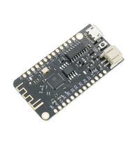
WEMOS LOLIN32 Lite Development Board Pinout and Technical Specifications
Code name: LOLIN32_LITE
Manufacturer: Wemos
WEMOS LOLIN32 Lite development board is based on esp32 microcontroller and uses xtensa architecture. This development board has a maximum CPU frequency of 240 MHz and a flash size of 4MB.
🔗 Quick Links
📊 WEMOS LOLIN32 Lite Specs
Below you can find the specifications of WEMOS LOLIN32 Lite, such as features, connectivity options, and WEMOS LOLIN32 Lite technical specs.
✨ Features
- 40 digital IO pins
- 16 external interrupt pins
- 16 analog input pins
- 18 PWM pins
🛰️ Connectivity
- WiFi: 802.11 b/g/n (2.4 GHz)
- Bluetooth: 4.2
- BLE: 4.2
📐 Technical specs
| Microcontroller | esp32 |
| Clock Speed | 240 MHz |
| Flash size | 4MB |
| Architecture | xtensa |
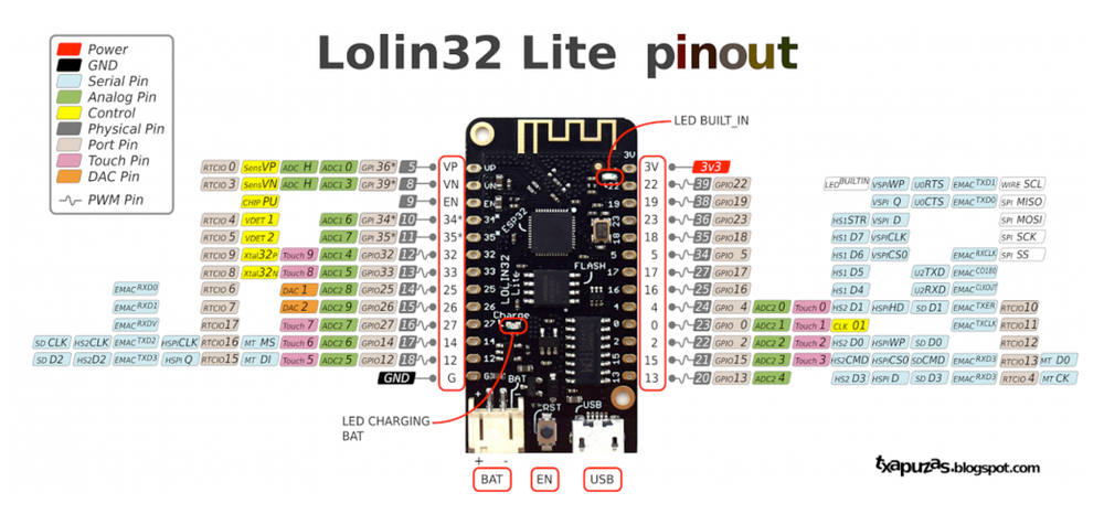
🔌 WEMOS LOLIN32 Lite Pinout
⚠️ Pins to Avoid or Use with Caution
Some pins are reserved for critical functions like bootstrapping, JTAG debugging, USB communication, and flash memory operations. Misusing these pins may lead to boot failures, programming issues, USB conflicts, or disruptions in flash storage. Below is a list of pins to avoid or use with caution, categorized for clarity:
- 🛠️ Strapping Pins (Boot Mode & System Behavior) - These pins control boot behavior and flash voltage selection. Pulling them high or low at reset can impact boot mode selection, voltage settings, or debugging access. Avoid altering their state unless necessary.
- 🔗 JTAG Debugging Pins - JTAG is used for low-level debugging and programming. If JTAG is enabled, these pins must remain dedicated to it. Repurposing them as GPIO can disable JTAG debugging features.
- 🔌 USB Communication Pins - These pins are used for USB Serial/JTAG communication. If USB debugging or communication is required, they should not be reassigned as GPIO.
- ⚡ Flash Memory & SPI Pins - Certain GPIOs are hardwired to SPI flash memory and PSRAM. Using them as standard GPIOs may result in system instability, corrupted storage, or boot failure.
- 📡 UART Serial Communication Pins - By default, these pins are used for serial debugging, console output, and firmware uploads. Repurposing them for general I/O may break UART programming or debugging capabilities.
| PIN | Label | Reason | Function |
|---|---|---|---|
| IO0 | GPIO0 | Must be HIGH during boot for normal startup; if held LOW on reset, forces flash programming mode. | 🛠️ Strapping |
| IO2 | GPIO2 | If driven HIGH on reset (while IO0 is LOW), selects an unsupported SDIO boot mode, causing boot failure. | 🛠️ Strapping |
| IO4 | GPIO4 | Sampled at reset for boot config; should not be driven at boot (affects boot mode timing). | 🛠️ Strapping |
| IO5 | GPIO5 | Must be HIGH during boot; if pulled LOW at reset, alters SDIO slave timing and may prevent normal boot. | 🛠️ Strapping |
| IO12 | MTDI (GPIO12) | Keep LOW during boot (internal PD); pulling HIGH at reset selects 1.8V flash mode, causing flash brownout if 3.3V flash is used. | 🛠️ Strapping |
| IO13 | MTCK (GPIO13) | Used for JTAG debugging (TCK); avoid using as GPIO if JTAG is needed. | 🪛 Other |
| IO14 | MTMS (GPIO14) | Used for JTAG debugging (TMS); driving it as GPIO may interfere with JTAG or produce spurious signals at boot. | 🪛 Other |
| IO15 | MTDO (GPIO15) | Keep HIGH during boot (internal PU); if LOW on reset, bootloader log is silenced and boot mode may change. | 🛠️ Strapping |
| IO16 | GPIO16 | Connected to internal PSRAM on PSRAM-enabled modules; not usable as GPIO on those modules. | ⚡ Flash |
| IO17 | GPIO17 | Connected to internal PSRAM on PSRAM-enabled modules; not usable as GPIO on those modules. | ⚡ Flash |
| IO34 | GPIO34 | Cannot be used as output (no drive capability); only suitable for analog/digital input. | 🪛 Other |
| IO35 | GPIO35 | Cannot be used as output; only suitable for input. | 🪛 Other |
| IO36 | GPIO36 (SENSOR_VP) | Cannot be used as output; only suitable for input (e.g., analog read). | 🪛 Other |
| IO39 | GPIO39 (SENSOR_VN) | Cannot be used as output; only suitable for input. | 🪛 Other |
📌 Key Takeaway:
- Before using any GPIO, check if it is assigned a critical function.
- Avoid using bootstrapping pins unless you're modifying boot behavior intentionally.
- If JTAG debugging is needed, ensure its pins remain free.
- USB and Flash-related GPIOs should remain dedicated unless you disable their default functions.
✅ Pins Safe to use
- 🔹 IO18
- 🔹 IO19
- 🔹 IO22
- 🔹 IO23
- 🔹 IO25
- 🔹 IO26
- 🔹 IO27
- 🔹 IO32
- 🔹 IO33
Unlike restricted pins, these GPIOs are not tied to essential system functions like 🛠️ bootstrapping, 🔌 USB communication, 🔗 JTAG debugging, or ⚡ SPI flash memory, making them the best choices for custom applications and general use.
Why Are These Pins Safe?- Not involved in bootstrapping → These GPIOs do not affect the device’s boot mode or system startup.
- Not linked to flash memory or PSRAM → They won’t interfere with storage or memory access.
- Not dedicated to USB or JTAG → They remain free for general use without affecting debugging or programming.
- No special hardware connections → Unlike some pins that are internally wired to system functions, these remain freely assignable.
🗺️ WEMOS LOLIN32 Lite External Pins Mapping Functions
Below you can find the WEMOS LOLIN32 Lite pinout. This development board provides 40 digital IO pins, out of which 16 can be used as an external interrupt pins , 16 as analog input pins and 18 pins have Pulse-Width Modulation (PWM) .
| Pin | Function | ESP Pin | Input/Output | Description |
|---|---|---|---|---|
| 1 | 5V | 5V | POWER INPUT | 5V power input for the board |
| 2 | GND | GND | POWER GROUNT | Ground connection |
| 3 | 3V3 | 3.3V | POWER OUTPUT | 3.3V power output |
| 5 | IO0 | GPIO0 | BIDIRECTIONAL | GPIO, ADC |
| 6 | IO2 | GPIO2 | BIDIRECTIONAL | GPIO, ADC |
| 7 | IO4 | GPIO4 | BIDIRECTIONAL | GPIO, ADC |
| 8 | IO5 | GPIO5 | BIDIRECTIONAL | GPIO |
| 9 | IO12 | GPIO12 | BIDIRECTIONAL | GPIO, ADC |
| 10 | IO13 | GPIO13 | BIDIRECTIONAL | GPIO, ADC |
| 11 | IO14 | GPIO14 | BIDIRECTIONAL | GPIO, ADC |
| 12 | IO15 | GPIO15 | BIDIRECTIONAL | GPIO |
| 13 | IO16 | GPIO16 | BIDIRECTIONAL | GPIO |
| 14 | IO17 | GPIO17 | BIDIRECTIONAL | GPIO |
| 15 | IO18 | GPIO18 | BIDIRECTIONAL | GPIO |
| 16 | IO19 | GPIO19 | BIDIRECTIONAL | GPIO |
| 17 | IO22 | GPIO22 | BIDIRECTIONAL | GPIO |
| 18 | IO23 | GPIO23 | BIDIRECTIONAL | GPIO |
| 19 | IO25 | GPIO25 | BIDIRECTIONAL | GPIO, ADC |
| 20 | IO26 | GPIO26 | BIDIRECTIONAL | GPIO, ADC |
| 21 | IO27 | GPIO27 | BIDIRECTIONAL | GPIO, ADC |
| 22 | IO32 | GPIO32 | BIDIRECTIONAL | GPIO, ADC |
| 23 | IO33 | GPIO33 | BIDIRECTIONAL | GPIO, ADC |
| 24 | IO34 | GPIO34 | BIDIRECTIONAL | GPIO, ADC |
| 25 | IO35 | GPIO35 | BIDIRECTIONAL | GPIO, ADC |
| 26 | IO36 | GPIO36 | BIDIRECTIONAL | GPIO, ADC |
| 27 | IO39 | GPIO39 | BIDIRECTIONAL | GPIO, ADC |
🗺️ WEMOS LOLIN32 Lite Pins Mapping Arduino IDE
Below you can find the WEMOS LOLIN32 Lite pinout. This development board provides 40 digital IO pins, out of which 16 can be used as an external interrupt pins , 16 as analog input pins and 18 pins have Pulse-Width Modulation (PWM) .
| Pin | Analog | Touch | PWM | Other |
|---|---|---|---|---|
| 0 | A11 | T1 | ||
| 1 | PWM | TX | ||
| 2 | A12 | T2 | PWM | |
| 3 | PWM | RX | ||
| 4 | A10 | T0 | PWM | |
| 5 | PWM | SS | ||
| 12 | A15 | T5 | PWM | |
| 13 | A14 | T4 | PWM | |
| 14 | A16 | T6 | PWM | |
| 15 | A13 | T3 | PWM | |
| 18 | PWM | SCK | ||
| 19 | PWM | SDA MISO | ||
| 22 | PWM | LED_BUILTIN | ||
| 23 | PWM | SCL MOSI | ||
| 25 | A18 | PWM | DAC1 | |
| 26 | A19 | PWM | DAC2 | |
| 27 | A17 | T7 | PWM | |
| 32 | A4 | T9 | PWM | |
| 33 | A5 | T8 | PWM | |
| 34 | A6 | |||
| 35 | A7 | |||
| 36 | A0 | |||
| 39 | A3 |
🛠️ Default Tools
| Bootloader tool | esptool_py |
| Uploader tool | esptool_py |
| Network uploader tool | esp_ota |
| Bootloader address | 0x1000 |
| Flash mode | dio |
| Boot mode | dio |
| PSRAM type | |
| Maximum upload size | 1280 Kb (1310720 B) |
| Maximum data size | 320 Kb (327680 B) |
The WEMOS LOLIN32 Lite development board by default uses esptool_py uploader tool, esp_ota network uploader tool for Over-the-air (OTA) uploads and esptool_py bootloader tool. The bootloader starts at address "0x1000". Flash mode and boot mode for WEMOS LOLIN32 Lite development board by default is dio and dio respectively.