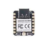
Seed Studio XIAO ESP32C3 (XIAO ESP32C3 ) Development Board Pinout and Technical Specifications
Code name: XIAO_ESP32C3
Manufacturer: Seed Studio
Seed Studio XIAO ESP32C3 (XIAO ESP32C3) development board is based on esp32c3 microcontroller and uses riscv32 architecture. This development board has a maximum CPU frequency of 160 MHz and a flash size of 4MB.
🔗 Quick Links

🛒 Price


📝 XIAO ESP32C3 Description
The XIAO ESP32C3 is a compact and versatile development board based on the ESP32-C3 RISC-V chip. With built-in WiFi 802.11b/g/n and Bluetooth 5 (LE), it is ideal for IoT applications requiring wireless communication. 📡
Its small form factor makes it suitable for wearable projects, DIY automation, and more. The board features a USB-C port for easy programming and power supply. It supports multiple communication interfaces, including UART, I2C, and SPI. 🚀
The XIAO ESP32C3 also includes a reset button and a bootloader mode button, simplifying development and debugging.⚡
📊 XIAO ESP32C3 Specs
Below you can find the specifications of XIAO ESP32C3, such as features, connectivity options, and XIAO ESP32C3 technical specs.
✨ Features
- Ultra-small form factor (20x17.5 mm)
- Low power consumption with deep sleep support
- 11 digital IO pins
- 11 external interrupt pins
- 3 analog input pins
- 11 PWM pins
🔌 USB
- Type: USB-C
- Chip: Internal
🛰️ Connectivity
- WiFi: 802.11 b/g/n (2.4 GHz)
- Bluetooth: 5.0
- BLE: 5.0
📐 Technical specs
| Microcontroller | esp32c3 |
| Clock Speed | 160 MHz |
| Flash size | 4MB |
| SRAM Size | 400KB |
| Architecture | riscv32 |
🔌 XIAO ESP32C3 Pinout
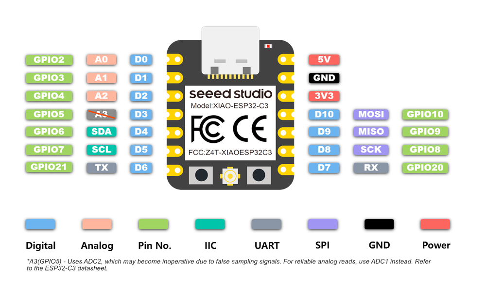
The XIAO ESP32C3 pinout is optimized for maximum functionality in a tiny package. It includes essential power pins like 5V, 3.3V, and GND for stable power delivery.
It supports multiple communication protocols, with dedicated pins for UART (RX and TX), I2C (SDA and SCL), and SPI (SCK, MISO, MOSI, and SS).
Analog input pins are labeled A0 to A3, making them ideal for sensor integration. Despite its small size, the XIAO ESP32C3 provides flexible connectivity for a variety of applications.
⚠️ Pins to Avoid or Use with Caution
Some pins are reserved for critical functions like bootstrapping, JTAG debugging, USB communication, and flash memory operations. Misusing these pins may lead to boot failures, programming issues, USB conflicts, or disruptions in flash storage. Below is a list of pins to avoid or use with caution, categorized for clarity:
- 🛠️ Strapping Pins (Boot Mode & System Behavior) - These pins control boot behavior and flash voltage selection. Pulling them high or low at reset can impact boot mode selection, voltage settings, or debugging access. Avoid altering their state unless necessary.
- 🔗 JTAG Debugging Pins - JTAG is used for low-level debugging and programming. If JTAG is enabled, these pins must remain dedicated to it. Repurposing them as GPIO can disable JTAG debugging features.
- 🔌 USB Communication Pins - These pins are used for USB Serial/JTAG communication. If USB debugging or communication is required, they should not be reassigned as GPIO.
- ⚡ Flash Memory & SPI Pins - Certain GPIOs are hardwired to SPI flash memory and PSRAM. Using them as standard GPIOs may result in system instability, corrupted storage, or boot failure.
- 📡 UART Serial Communication Pins - By default, these pins are used for serial debugging, console output, and firmware uploads. Repurposing them for general I/O may break UART programming or debugging capabilities.
| PIN | Label | Reason | Function |
|---|---|---|---|
| IO2 | GPIO2 | Must be held high during boot (if low on reset, normal flash boot may fail) | 🛠️ Strapping |
| IO4 | MTMS | Used during boot; JTAG TMS for debugging; acts as Quad-SPI flash IO (hold data line) in internal-flash variants | 🔗 JTAG |
| IO5 | MTDI | Used during boot; JTAG TDI for debugging; acts as Quad-SPI flash IO (write-protect data line) in internal-flash variants | 🔗 JTAG |
| IO6 | MTCK | Used during boot; JTAG TCK for debugging; provides flash clock in internal-flash variants | 🔗 JTAG |
| IO7 | MTDO | Used during boot; JTAG TDO for debugging; acts as Quad-SPI flash IO (data line) in internal-flash variants | 🔗 JTAG |
| IO8 | GPIO8 | Must be held high during reset (if low, UART flashing/boot may not work) | 🛠️ Strapping |
| IO9 | GPIO9 | Controls boot mode on reset (HIGH for normal flash boot, LOW enters serial download mode) | 🛠️ Strapping |
| IO20 | U0RXD | Used as UART0 receive (console/bootloader); repurposing may disable serial programming and debug logs | 📡 UART |
| IO21 | U0TXD | Used as UART0 transmit (console/bootloader); repurposing may disable serial console output and printing | 📡 UART |
📌 Key Takeaway:
- Before using any GPIO, check if it is assigned a critical function.
- Avoid using bootstrapping pins unless you're modifying boot behavior intentionally.
- If JTAG debugging is needed, ensure its pins remain free.
- USB and Flash-related GPIOs should remain dedicated unless you disable their default functions.
✅ Pins Safe to use
- 🔹 IO3
- 🔹 IO10
Unlike restricted pins, these GPIOs are not tied to essential system functions like 🛠️ bootstrapping, 🔌 USB communication, 🔗 JTAG debugging, or ⚡ SPI flash memory, making them the best choices for custom applications and general use.
Why Are These Pins Safe?- Not involved in bootstrapping → These GPIOs do not affect the device’s boot mode or system startup.
- Not linked to flash memory or PSRAM → They won’t interfere with storage or memory access.
- Not dedicated to USB or JTAG → They remain free for general use without affecting debugging or programming.
- No special hardware connections → Unlike some pins that are internally wired to system functions, these remain freely assignable.
🗺️ XIAO ESP32C3 External Pins Mapping Functions
Below you can find the XIAO ESP32C3 pinout. This development board provides 11 digital IO pins, out of which 11 can be used as an external interrupt pins , 3 as analog input pins and 11 pins have Pulse-Width Modulation (PWM) .
| Pin | Function | ESP Pin | Input/Output | Description |
|---|---|---|---|---|
| 1 | 5V | 5V | POWER INPUT | 5V power input |
| 2 | GND | GND | GROUND | Ground connection |
| 3 | 3V3 | 3.3V | POWER OUTPUT | 3.3V power output |
| 4 | IO2 | A0 | BIDIRECTIONAL | GPIO, ADC |
| 5 | IO3 | A1 | BIDIRECTIONAL | GPIO, ADC |
| 6 | IO4 | A2 | BIDIRECTIONAL | GPIO, ADC |
| 7 | IO5 | A3 | BIDIRECTIONAL | GPIO, ADC |
| 8 | IO6 | SDA | BIDIRECTIONAL | GPIO, I2C Data |
| 9 | IO7 | SCL | BIDIRECTIONAL | GPIO, I2C Clock |
| 10 | IO8 | SCK | BIDIRECTIONAL | GPIO, SPI Clock |
| 11 | IO9 | MISO | BIDIRECTIONAL | GPIO, SPI Data |
| 12 | IO10 | MOSI | BIDIRECTIONAL | GPIO, SPI Data |
| 13 | IO20 | RX | BIDIRECTIONAL | GPIO, UART Receive |
| 14 | IO21 | TX | BIDIRECTIONAL | GPIO, UART Transmit |
🗺️ XIAO ESP32C3 Pins Mapping Arduino IDE
Below you can find the XIAO ESP32C3 pinout. This development board provides 11 digital IO pins, out of which 11 can be used as an external interrupt pins , 3 as analog input pins and 11 pins have Pulse-Width Modulation (PWM) .
| Pin | Analog | Touch | PWM | Other |
|---|---|---|---|---|
| 2 | A0 | |||
| 3 | A1 | |||
| 4 | A2 | |||
| 5 | A3 | |||
| 6 | SDA | |||
| 7 | SCL | |||
| 8 | SCK | |||
| 9 | MISO | |||
| 10 | MOSI | |||
| 20 | RX SS | |||
| 21 | TX |
🛠️ Default Tools
| Bootloader tool | esptool_py |
| Uploader tool | esptool_py |
| Network uploader tool | esp_ota |
| Bootloader address | 0x0 |
| Flash mode | qio |
| Boot mode | qio |
| PSRAM type | |
| Maximum upload size | 1280 Kb (1310720 B) |
| Maximum data size | 320 Kb (327680 B) |
The XIAO ESP32C3 development board by default uses esptool_py uploader tool, esp_ota network uploader tool for Over-the-air (OTA) uploads and esptool_py bootloader tool. The bootloader starts at address "0x0". Flash mode and boot mode for XIAO ESP32C3 development board by default is qio and qio respectively.