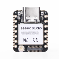
XIAO ESP32S3 Plus Development Board Pinout and Technical Specifications
Code name: XIAO_ESP32S3_PLUS
Manufacturer: Seed Studio
XIAO ESP32S3 Plus development board is based on esp32s3 microcontroller and uses xtensa architecture. This development board has a maximum CPU frequency of 240 MHz and a flash size of 16MB.
🔗 Quick Links

🛒 Price


📝 XIAO ESP32S3 Plus Description
The XIAO ESP32S3 Plus is a high-performance development board based on the ESP32-S3 dual-core processor with enhanced features. It supports WiFi 4 and Bluetooth 5 (LE), making it ideal for IoT, AI, and embedded applications. 📡
With a compact yet powerful design, it includes a USB-C port for fast programming and power, and features additional onboard peripherals such as an integrated accelerometer and external memory support. ⚡
The XIAO ESP32S3 Plus supports multiple communication interfaces, including UART, I2C, SPI, and ADC, making it a great choice for advanced embedded applications.
📊 XIAO ESP32S3 Plus Specs
Below you can find the specifications of XIAO ESP32S3 Plus, such as features, connectivity options, and XIAO ESP32S3 Plus technical specs.
✨ Features
- Dual-core Xtensa LX7 processor with enhanced AI capabilities
- Integrated accelerometer and external memory support
- Supports WiFi 4 and Bluetooth 5 (LE)
- Ultra-small size (21x17.5 mm)
- 18 digital IO pins
- 18 external interrupt pins
- 9 analog input pins
- 18 PWM pins
🔌 USB
- Type: USB-C
🛰️ Connectivity
- WiFi: 802.11 b/g/n (2.4 GHz)
- Bluetooth: 5.0
- BLE: 5.0
📐 Technical specs
| Microcontroller | esp32s3 |
| Clock Speed | 240 MHz |
| Flash size | 16MB |
| PSRAM Size | 8MB |
| Architecture | xtensa |
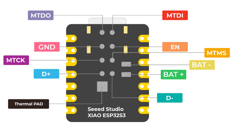
🔌 XIAO ESP32S3 Plus Pinout
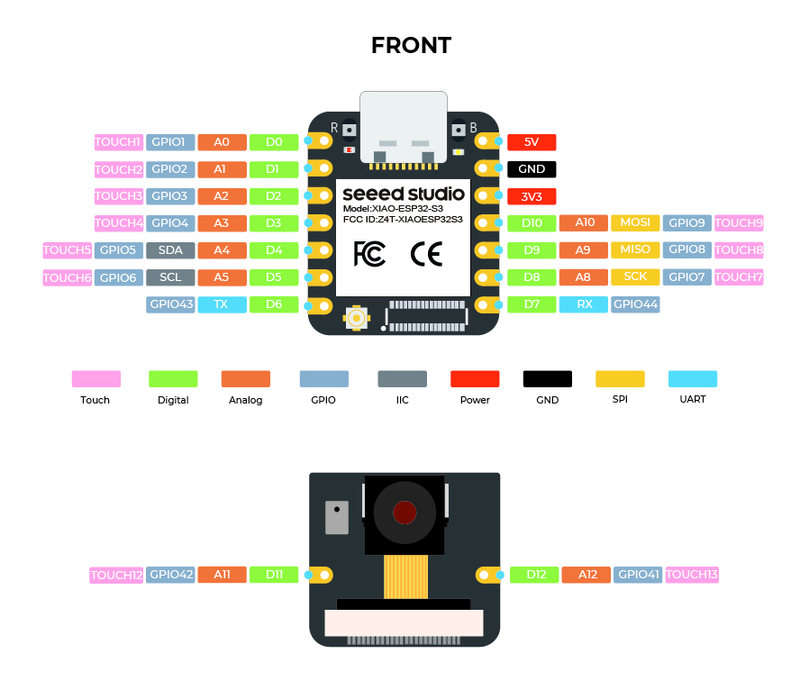
The XIAO ESP32S3 Plus pinout is designed for expanded functionality and includes additional peripheral connections. It features key power pins like 5V, 3.3V, and GND for stable power delivery.
It supports multiple communication protocols, including UART (RX and TX), I2C (SDA and SCL), and SPI (SCK, MISO, MOSI, and SS).
Analog input pins labeled A0 to A3 enable sensor integration, while additional GPIOs provide further expandability.
⚠️ Pins to Avoid or Use with Caution
Some pins are reserved for critical functions like bootstrapping, JTAG debugging, USB communication, and flash memory operations. Misusing these pins may lead to boot failures, programming issues, USB conflicts, or disruptions in flash storage. Below is a list of pins to avoid or use with caution, categorized for clarity:
- 🛠️ Strapping Pins (Boot Mode & System Behavior) - These pins control boot behavior and flash voltage selection. Pulling them high or low at reset can impact boot mode selection, voltage settings, or debugging access. Avoid altering their state unless necessary.
- 🔗 JTAG Debugging Pins - JTAG is used for low-level debugging and programming. If JTAG is enabled, these pins must remain dedicated to it. Repurposing them as GPIO can disable JTAG debugging features.
- 🔌 USB Communication Pins - These pins are used for USB Serial/JTAG communication. If USB debugging or communication is required, they should not be reassigned as GPIO.
- ⚡ Flash Memory & SPI Pins - Certain GPIOs are hardwired to SPI flash memory and PSRAM. Using them as standard GPIOs may result in system instability, corrupted storage, or boot failure.
- 📡 UART Serial Communication Pins - By default, these pins are used for serial debugging, console output, and firmware uploads. Repurposing them for general I/O may break UART programming or debugging capabilities.
| PIN | Label | Reason | Function |
|---|---|---|---|
| IO3 | GPIO3 | Sampled at reset to select JTAG interface (USB Serial/JTAG controller vs. external pins). Improper use can disable external JTAG or alter debug interface. | 🛠️ Strapping |
| IO9 | FSPIHD | Connected to external flash (data/hold signal) on most modules. Not recommended for use as GPIO, since it must remain dedicated to flash communication. | ⚡ Flash |
| IO10 | FSPICS0 | Used to select the external flash chip. It is required for flash access and cannot be repurposed without losing flash connectivity | ⚡ Flash |
| IO20 | USB_D+ | By default connected to the on-chip USB Serial/JTAG controller. Using it as general GPIO without reconfiguring IO MUX will interfere with USB functionality. | 🔌 USB |
📌 Key Takeaway:
- Before using any GPIO, check if it is assigned a critical function.
- Avoid using bootstrapping pins unless you're modifying boot behavior intentionally.
- If JTAG debugging is needed, ensure its pins remain free.
- USB and Flash-related GPIOs should remain dedicated unless you disable their default functions.
✅ Pins Safe to use
- 🔹 IO2
- 🔹 IO4
- 🔹 IO5
- 🔹 IO6
- 🔹 IO7
- 🔹 IO8
- 🔹 IO21
Unlike restricted pins, these GPIOs are not tied to essential system functions like 🛠️ bootstrapping, 🔌 USB communication, 🔗 JTAG debugging, or ⚡ SPI flash memory, making them the best choices for custom applications and general use.
Why Are These Pins Safe?- Not involved in bootstrapping → These GPIOs do not affect the device’s boot mode or system startup.
- Not linked to flash memory or PSRAM → They won’t interfere with storage or memory access.
- Not dedicated to USB or JTAG → They remain free for general use without affecting debugging or programming.
- No special hardware connections → Unlike some pins that are internally wired to system functions, these remain freely assignable.
🗺️ XIAO ESP32S3 Plus External Pins Mapping Functions
Below you can find the XIAO ESP32S3 Plus pinout. This development board provides 18 digital IO pins, out of which 18 can be used as an external interrupt pins , 9 as analog input pins and 18 pins have Pulse-Width Modulation (PWM) .
| Pin | Function | ESP Pin | Input/Output | Description |
|---|---|---|---|---|
| 1 | 5V | 5V | POWER INPUT | 5V power input |
| 2 | GND | GND | GROUND | Ground connection |
| 3 | 3V3 | 3.3V | POWER OUTPUT | 3.3V power output |
| 4 | IO2 | A0 | BIDIRECTIONAL | GPIO, ADC |
| 5 | IO3 | A1 | BIDIRECTIONAL | GPIO, ADC |
| 6 | IO4 | A2 | BIDIRECTIONAL | GPIO, ADC |
| 7 | IO5 | A3 | BIDIRECTIONAL | GPIO, ADC |
| 8 | IO6 | SDA | BIDIRECTIONAL | GPIO, I2C Data |
| 9 | IO7 | SCL | BIDIRECTIONAL | GPIO, I2C Clock |
| 10 | IO8 | SCK | BIDIRECTIONAL | GPIO, SPI Clock |
| 11 | IO9 | MISO | BIDIRECTIONAL | GPIO, SPI Data |
| 12 | IO10 | MOSI | BIDIRECTIONAL | GPIO, SPI Data |
| 13 | IO20 | RX | BIDIRECTIONAL | GPIO, UART Receive |
| 14 | IO21 | TX | BIDIRECTIONAL | GPIO, UART Transmit |
🛠️ Default Tools
| Bootloader tool | esptool_py |
| Uploader tool | esptool_py |
| Network uploader tool | esp_ota |
| Bootloader address | 0x0 |
| Flash mode | qio |
| Boot mode | qio |
| PSRAM type | |
| Maximum upload size |
8192 Kb
(8388608 B)
|
| Maximum data size |
320 Kb
(327680 B)
|
The XIAO ESP32S3 Plus development board by default uses esptool_py uploader tool, esp_ota network uploader tool for Over-the-air (OTA) uploads and esptool_py bootloader tool. The bootloader starts at address "0x0". Flash mode and boot mode for XIAO ESP32S3 Plus development board by default is qio and qio respectively.